

.svg)
AI Chips: A Practical Engineering Guide to How Modern Neural Processors Really Work
AI Chips: A Practical Engineering Guide to How Modern Neural Processors Really Work

Most content about AI chips oversimplifies everything. You'll see the same recycle lines about "chips designed for artificial intelligence" and lists of acronyms with no real explanation. None of that helps you understand how these processors actually run neural networks or why different architectures behave so differently in real workloads.
This is meant to fix that. It explains AI chips from the perspective of someone who has built and deployed them, not someone repeating marketing language. The goal is to give engineers a clear mental model of what is happening inside the silicon.
What an AI chip really is
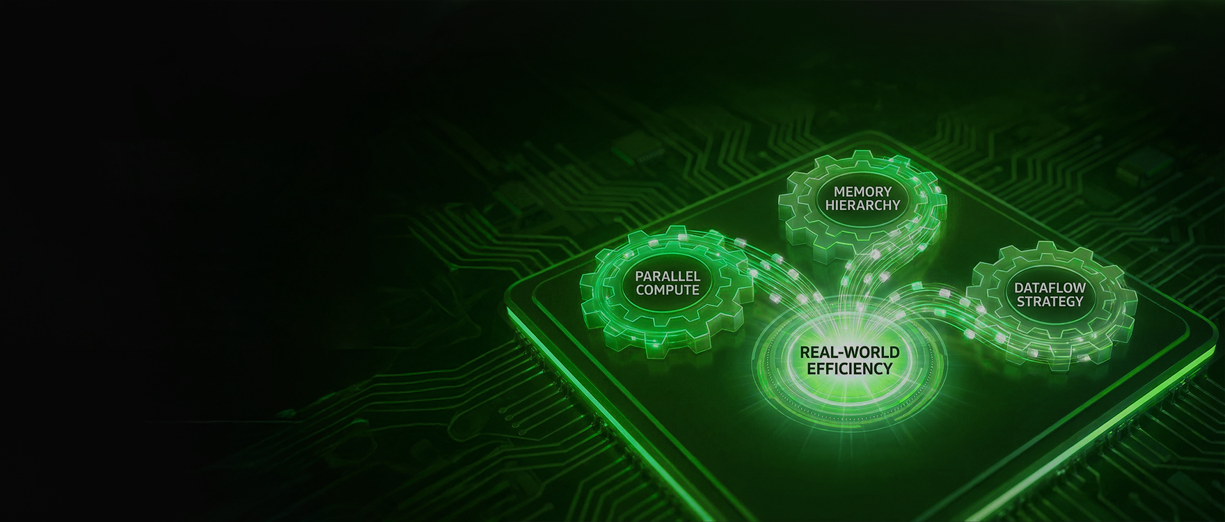
An AI chip is a processor built to execute neural networks operations with higher efficiency than a general-purpose CPU. It does this by combining three things:
- Highly parallel compute units
- A memory hierarchy that keeps data close to the compute
- A dataflow strategy that controls how weights and activations move through the system
If you understand those three components, you understand the design philosophy behind every modern AI chip.
The compute fabric explained
Neural networks rely heavily on matrix multiplications and convolutional operations. These operations map perfectly onto architectures with:
- Multiply accumulate (MAC) arrays
- Vector processing units
- Tensor cores
- In-Memory compute cells in analog or mixed-signal designs
The goal is simple. Instead of processing values on at a time, the chip processes many elements in parallel.
A common mistake in assuming the size of the MAC array determines real performance. It does not. Utilization matters far more. A large array is useless if it is constantly waiting for data.
Why memory hierarchy decides everything
This is the part most articles gloss over, but it is the part that determines whether a chip performs well under load.
Modern AI chips use a layered memory structure:
- Small local registers
- Larger SRAM buffers
- L2 or unified on-chip memory
- Optional off-chip DRAM
- External I/O or flash storage
Every layer has different latency and power characteristics. The more often the chip needs the move data between layers, the worse the performance becomes.
Moving data often costs more energy than the compute itself. This is why architectures that reuse data in place and reduce memory movement outperform chips that rely on constant DRAM access.
The importance of dataflow
Every AI chip has a dataflow pattern that defines how data moves through the compute units. Some common strategies include:
- Weight stationary
- Output stationary
- Row stationary
- Input stationary
- In-Memory compute
Dataflow is not marketing jargon. It has real consequences.
A weight stationary design keeps weights local so inputs flow through the compute. An output stationary design keeps partial results inside the array. In-memory compute keeps both weights and activations inside the storage elements, minimizing movement.
The right dataflow can save power, improve latency and increase utilization. The wrong one stall the entire pipeline.
Precision formats and why they matter
AI chip often use lower precision formats:
- FP16
- INT8
- INT4
- Binary or analog values in some mixed-signal designs
Lower precision reduces memory footprint and energy consumption, which is crucial for edge devices. The challenge is retaining accuracy while operating with smaller numerical ranges. Good compilers and quantization techniques solve part of this, but architecture also plays a major role.
What separates cloud AI chips from edge AI chips
Cloud-first accelerators are designed for throughput. They expect:
- High batch sizes
- Large DRAM bandwidth
- High power budgets
- Adequate cooling
- Flexible memory management
They scale extremely well for training and large-batch inference. They do not scale down to the edge easily.
Edge AI chips face constraints cloud silicon never does. They must:
- Operate at milliwatt or microwatt power
- Handle real-silicon input
- Run at batch size equal to 1
- Avoid DRAM dependency
- Meet strict latency requirements
- Fit inside small form factors
This forces architectural decisions that prioritize data locality and continuous operation.
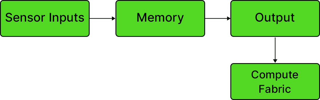
How AI chips handle sensor-driven workloads
Most Edge intelligence starts with raw sensor data:
- Audio
- IMU readings
- ECG or PPG waveforms
- Low-resolution vision inputs
A practical AI chip needs more than a neural network engine. It needs:
- DSP blocks
- Sensor interfaces
- Always-on wake pipelines
- Lightweight preprocessing stages
This is the part many "AI chips" overlook. They assume a clean tensor arrives ready for inference. Real devices never work like that.
A complement edge AI chip must ingest unstructured sensor data and prepare it for neural processing without waking an external MCU unnecessarily.
Why compute in memory is becoming important
Architectures relying on DRAM or large caches face a hard scaling limit. As models shrink for edge use, memory movement becomes an even larger fraction of total energy consumption.
Compute-in-memory architectures change this by reducing the distance data travels. They embed computation into the memory fabric itself so weights do not need to be constantly fetched.
This approach:
- Cuts energy consumption
- Reduces latency
- Improves compute density
- Reduces external memory dependency
It is becoming one of the most promising approaches for low-power, always-on edge AI.
How to evaluate an AI chip intelligently
A practical engineer does not look at TOPs numbers. They ask the following:
- Can the model fit in on-chip memory without DRAM access
- How many times does the data move during inference
- What is the sustained performance at batch size equal to 1
- What is the always-on power for continuous workloads.
- Does the pipelines requires a separate MCU for preprocessing.
- How well does the chip handle sensor-driven data.
- What dataflow architecture is used.
- Does the compiler optimized model layout for the hardware.
These are the questions that decide real-world feasibility.
The bottom line
AI chips only make sense when you understand how the compute units, memory hierarchy and dataflow interact. Modern neural processors are not magic. They are carefully engineered systems designed to minimize unnecessary and maximize useful work.
If you are building an edge AI product, your chip choice is going to define your power budget, latency, battery life, and user experience. Understanding how these processors work at a practical level is the difference between a device that operates for months and a device that drains itself in days.
If you want help evaluating architectures for your next products, reach out.
Contact Us


.png)

